| Diode side-pumped Solid-state lasers |
Diode-side-pumped high power CW Nd:YAG laser:
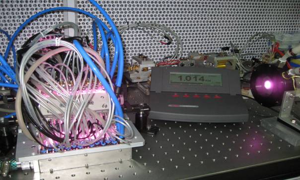
The major activities of this lab is to develop and engineer high power/high energy Nd:YAG laser for different applications. Towards these goals we also engaged in pursuing research on novel pumping geometries and techniques to improve the performance to its limits. Recently we have developed a very compact, high-power, diode-pumped kW-class CW Nd:YAG laser. The system consists of 0.6% doped Nd:YAG rod of 6 mm in diameter, 150 mm in length is surrounded by a copper-coated quartz flow tube on the outside surface with three narrow windows of 1.5 mm width and 125 mm long in threefold angularly symmetric directions for coupling the diode radiation. The reflecting coating over the flow tube traps the pump light within the flow tube by multiple reflections for efficient utilization of the pump radiation. We preferred copper metal film than gold for two reasons: a) copper has excellent adhesion on the glass substrate b) it has higher reflectivity than gold around the diode emission at 800nm. Pumping is performed by total 30 nos of 80 Watts laser diode bars grouped in a three linear modules. Diode pump modules are located 0.5mm in front of the center of 3-fold symmetric windows to couple the diode beams into the flow tube. The laser resonator was formed by a plane high reflection rear mirror and 80% plane output coupler separated over a distance of 180mm. The maximum multimode laser output power of 1200W was achieved for the diode pump power of 2360W. This corresponds to an optical slope efficiency of 52% and an optical conversion efficiency of 48%. This is to the best of our knowledge, the highest output power reported for a 6 mm diameter Nd:YAG rod in CW diode-side-pumped Nd:YAG laser. Figure below shows the photograph of the laser in operation. The overall size of the laser head is 225x220x250mm3. This laser has potential for various industrial applications such as cutting, welding, surface hardening, and laser rapid prototyping. Fiber delivery for this laser using 600 micron core diameter fiber upto an output power at the fiber tip of 700W has been demonstrated.
 |
Photograph of the laser setup |
Slab geometry lasers:
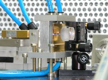
In conduction-cooled, edge-pumped slab laser geometries the efficient heat removal is affected by using water-cooled microchannel heat sinks made up of copper as base material. We have fabricated copper microbars by fine slit cutters. The performance in terms of thermal resistance was measured to be 0.3°C/W over the surface area of 10x40mm2. Studies on various kinds of slab geometry Nd:YAG laser setup has been pursued. Those include water-cooled thin slab, conduction-cooled edge-pumping as well as end-pumped schemes. We have achieved 250W multimode and 70W polarized single mode output using lens duct coupled diode stacks with 1.5x5x75mm3 Nd:YAG slab. In conduction cooled end pumped Nd:YAG laser setup 180W multimode power was achieved using 2x9x18mm crystal.
 |
Photograph of experimental setup of slab geometry laser |
Laser marker:
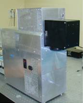
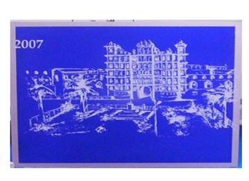
We have developed a compact laser marker system using end-pumped, Q-switched Nd:YVO4 laser. The maximum average and peak power is 5W and 40kW respectively. The scanning of the laser beam has been done by x-y scanner assembly with a flat field objective of 163mm focal length having marking field of 110x110mm2. The focused spot size is around 50µm and marking speed close to 1m/s can be achieved. Marking of photographs using raster scanning technique can also be made with high resolution.
|
 |
Photograph of the laser marker and a marked picture |
Selective Laser Melting (SLM) and micromachining using Nd:YAG laser:
Laser sintering is a process by which a three dimensional job can be created by melting metal powders, selectively by layer-by-layer using CAD data. Particularly nickel-based alloy, Fe alloy and pure titanium powders are found to be feasible for fabrication of metallic models by SLM. A CW Nd: YAG laser with a maximum power of 70 W has been developed to melt metallic powders. The three-dimensional model is built on the base plate by deflecting the laser beam using x-y scan head controlled with a PC. The processing with the laser beam is carried out in the chamber filled with inactive gas such as argon and nitrogen to avoid oxidation. This process allows greater flexibility in creating individualized products in a cheaper and faster way. At SSLD we have developed a laser which is integrated with x-y scanners. We have attempted to build components on SS powder and the results are encouraging. Using the same laser with high repetition acousto optic Q-switching high peak power laser pulses can be generated in sub-micro second pulsedurations for micromachining applications.
|
| |
|


